FPGA DSP radio for narrow band communications [ 150177-I ]

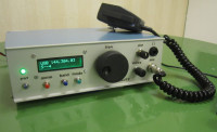
I am working on a complete high performance transceiver for narrow band SSB/CW (and possibly also AM and FM) on shortwave and/or VHF (amateur radio bands) based on signal processing in an FPGA together with 24 bit ADC and a very fast DAC.It is stand-alone and not like most other SDR projects that are relying on a PC.
I am working on a complete high performance transceiver for narrow band SSB/CW (and possibly also AM and FM) on shortwave and/or VHF (amateur radio bands) based on signal processing in an FPGA together with 24 bit ADC and a very fast DAC.
It is stand-alone and not like most other SDR projects that are relying on a PC.
See https://www.youtube.com/watch?v=BCwOSmN_0kI for a working demo.
At https://sm6vfz.wordpress.com/dspsdr-with-fpga/ there is a draft project log book with some pictures. RF circuitry, including LO synthesizer, is also being built from scratch.
From the lab: FPGA DSP Board for Narrow-band Radio
Thanks to Daniel we’re able to present a brilliant design. Let’s be honest, all credit goes to Daniel. We designed the PCBs with guidance and corrections from Daniel. We started this project at the end of 2015, this may seem like a long time but now we really have something to show for.
(Text by Daniel)
Abstract
This project presents a board for high-performance, narrow-band, radio operation. It features a 24 bit ADC for sampling at intermediate frequency in receive mode, a Cyclone IV FPGA for signal processing, a high-speed DAC for local oscillator and transmit signal generation, an audio coded for digital-to-mic/speaker, a TCXO for high frequency stability and an I2C or UART interface for a host controller. A simple radio front-end board is also presented, with which one can build a transceiver for shortwave easily
Circuit description
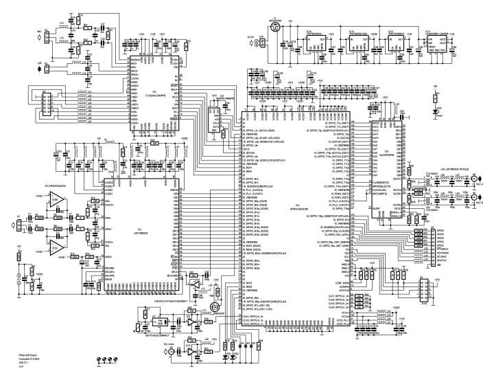
The heart (or brain) of the board consists of the EP4CE10 Cyclone IV FPGA from Intel, formerly Altera (IC4). This is a chip that can be configured for virtually any digital function. Its gates are connected at start-up according to the firmware in an external flash (IC5) that is known as the configuration memory.

For audio input and output there is a “codec”, TLV320AIC20K (IC3), which consists of dual ADC's and DAC's at 16 bit resolution and maximum 25 ksps. It incorporates a digital 8 kHz low pass filter, as well as a mic amplifier and a speaker driver that can deliver 250mW into 8 Ohm. For all analog audio I/O's there are selectable gain/attenuation factors for volume control etc. Apart from connection to speaker (K2) and mic (K3), it has other channels connected at K4 that can be used for audio connection to auxiliary equipment.
The main input to the board is a differential signal typically in the hundreds of kHz-range, at K1. This passes a differential opamp amplifier (IC1) and a discrete filter, to finally be digitized in an AD7760 24 bit ADC (IC2). This chip has many supply connections, which are separated by voltage and/or passive filtering. Its master clock comes from the FPGA and is amplified to 5V swing by IC8.
There is also a fast two-channel DAC on the board, DAC5672 (IC6) with output transformers, for differential to single-ended, and low pass filtering that lets through signals up to 50 MHz. Its two output channels, called A and B, are available at K8 and K9.
To clock everything a 20 MHz TCXO (IC7) is on the board. This clock is fed to the FPGA and then redistributed to the peripheral ICs. The frequency can be fine-tuned with potentiometer P1. There is also an input for an external reference source when that is available (K5). Depending on the availability of an external reference, the TCXO can be turned on or off through T1. Both the signal from the TCXO and the external reference are fed to the FPGA through unbuffered inverters connected for analog amplification (IC9, IC10). These signals can then be of moderate voltage swing.
The clock is divided down in the FPGA to generate a low frequency flash in LED1, indicating that the clock is running and the FPGA is configured.
A supply voltage of 5V, coming in at K10, is distributed to four different LDO's (IC11-14) to generate the voltages necessary for the different chips, at 1.2V, 1.8V, 2.5V and 3.3V The interface to the host controller consists of two pins intended for I2C or UART communication, selectable by solder jumper (JP1). There are also seven additional GPIOs (at K7) used typically for PTT (Push-to-talk) and Morse key signals. It should also be possible to use these pins for I2S audio I/O.
In addition there is a JTAG interface for programming of the FPGA and its configuration memory (K6).
Programming
The compiled firmware for this project, named “TRX”, is available as a “JTAG indirect configuration” file (trx.jic) that first configures the FPGA as a bridge and then programs the configuration memory through the former. This is done with the aid of an “USB Blaster” that connects to a PC over USB to form a JTAG interface to the board. Such a device can be bought very cheaply - look on eBay, AliExpress and similar sites. The software to use at the PC side is known as Quartus Lite and can be freely downloaded from the Intel/Altera website. If the complete development environment is not of interest then there is the possibility to download only the applications needed for programming. The Quartus suite is available both for Windows and Linux computers.
Control interface
In a stand-alone radio the controller would likely be a small microcontroller board with display and buttons. This could be designed with a PIC, AVR, STM32 or basically any other type of processor. It could also be a ready-made Arduino, Teensy, Platino or any other popular prototyping board. For experiments, or when a monitor and mouse/keyboard is not an obstacle, a Raspberry Pi makes a flexible control interface.
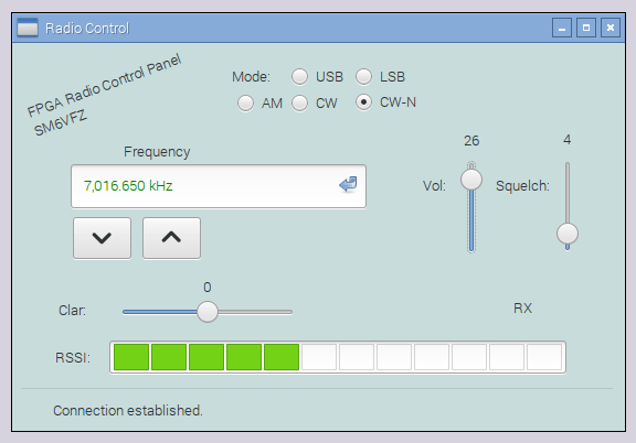
For the Raspberry Pi (or any other Linux computer), an applet was written in Python, with the GTK graphical framework, that makes the controls easily accessible. This applet connects to the FPGA board over UART serial port by default. It also has an experimental socket mode, to enable remote operation. The idea is then to run a server on a Raspberry Pi at the location of the radio and connect to this Pi with the applet from a remote computer.
With the large amount of man-made noise in urban areas, and with the limitations to installing large antennas in these locations, the option of remote operation becomes more and more interesting for radio amateurs and shortwave listeners.
It should also be possible to route the audio from the FPGA directly to the PCM/I2S ports of the Raspberry Pi in order to avoid the detour over analog audio when doing remote operation. This is yet to be tested.

Radio board
A design of a simple RF / radio board with few components that is satisfying the block diagram TBD above was also made.

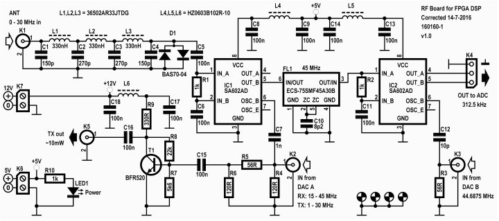
The antenna is connected at K1 where it sees a low-pass filter removing FM broadcast signals and other potential VHF/UHF interferers. The anti-parallel diode pair D1 limits very strong signals passing through the filter while it also provides a DC return path for static charge that otherwise can build up in a long and isolated antenna wire.
The well-proven SA602 chip (IC1) then amplifies the signal and mix it with the one coming from DAC A, at K2. A crystal filter, FL1, adds sharp filtering at the first intermediate frequency. The impedances of the SA602 and the filter match fairly well so no additional matching components (that normally would be needed) are used. Another SA602 then follows (IC2), which mix with the DAC B signal and produce the second IF as a differential signal (at K4) to be fed to the ADC of the FPGA board.
The RF and FPGA boards, together with a suitable controller for frequency selection etc., work very good for reception from virtually zero to around 30 MHz. When connected to a large antenna, that picks up both weak and strong signals, the receiver do not easily saturate and produce garbage audio like many other SDR solutions. It can therefore be used for serious work and reception of rare and weak signals.
Bill of materials FPGA DSP Board (150177-1 v2.1)
Resistor
R1,R2,R3,R4 = 560 Ω, 1 %, 0W1, SMD 0603
R5,R6,R25,R28,R30,R34,R35,R36,R44-R47,R48,R53 = 10 kΩ, 1 %, 0W1, SMD 0603
R7,R32,R33 = 330 Ω, 1 %, 0W1, SMD 0603
R8-R11,R19-R22,R37,R38,R39,R41 = 1 kΩ, 1 %, 0W1, SMD 0603
R12,R13 = 18 Ω, 1 %, 0W1, SMD 0603
R14,R17,R18 = 10 Ω, 1 %, 0W1, SMD 0603
R15,R49-R52,R54-R58 = 100 Ω, 1 %, 0W1, SMD 0603
R16 = 160 kΩ, 1 %, 0W1, SMD 0603
R23 = 47 kΩ, 1 %, 0W1, SMD 0603
R24,R29,R31 = 27 Ω, 1 %, 0W1, SMD 0603
R26 = 100 kΩ, 1 %, 0W1, SMD 0603
R27,R42,R43 = not mounted
R40 = 2k0, 1%, 0W1, SMD 0603
P1 = 10 kΩ, 20 %, trimmer, 4.5 mm, 250 mW, SMD (3314G-2-103E, Bourns)
Capacitor
C1,C2,C5-C8,C14,C16-C19,C20,C22,C23,C25,C27,C28,C29, C42,C44,C46,C47,C48,C50,C52,C53-C64,C66,C68,C70,C72,C73,C74,C75,C76,C77,C78,C79,C80,C81,C82,C92,C95,C98,C105,C106 = 100 nF, 10 %, 50 V, X7R, SMD 0603
C3,C4,C33,C34,C35 = not mounted
C9 = 5p6 ± 0.25 pF, 50 V, C0G/NP0, SMD 0603
C10,C11 = 27 pF, 1 %, 100 V, C0G/NP0, SMD 0603
C12,C21 = 10 nF, 10 %, 50 V, X7R, SMD 0603
C13,C43,C89,C90,C102,C103,C104,C107,C108,C109,C110 = 47 µF, 10 %, 16V, tantalum, 0.35 Ω, SMD Case C (TR3C476K016C0350, Vishay)
C15 = 33 pF, 5 %, 50 V, C0G/NP0, SMD 0603
C24,C26 = 10 µF, 10 %, 6V3, X7R, SMD 0805
C30,C31,C32 = 10 pF, 5 %, 50 V, C0G/NP0, SMD 0603
C36 = 1 nF, 10 %, 50 V, X7R, SMD 0603
C37,C38 = 22 nF, 10 %, 50 V, X7R, SMD 0603
C39,C40,C41,C93,C96,C99 = 1 µF, 10 %, 16 V, X7R, SMD 0603
C45,C49,C51 = 100 pF, 5 %, 50 V, C0G/NP0, SMD 0603
C83,C85,C86,C88 = 120 pF, 5 %, 50 V, C0G/NP0
C84,C87 = 180 pF, 5 %, 50 V, C0G/NP0, SMD 0603
C65,C67,C69,C71,C91,C94,C97,C100,C101 = 2µ2, 10 %, 6V3, X7R, SMD 0603
Inductor
L1,L2,L3,L4,L6,L7,L8,L9,L10,L11,L12,L13,L14,L15,L16,L17,L18,L19,L20,L21,L22,L23,L24,L25,L30,L31,L32,L33,L34,L35,L36,L37,L38,L39,L40 = 1 kΩ@100 MHz, 0Ω6, 200 mA, SMD 0603 (HZ0603B102R-10, Laird Technologies)
L5 = 15 nH, 5 %, 0Ω17, 700 mA, fres 4 GHz (CW160808-15NJ, Bourns)
L26,L27,L28,L29 = 180 nH, 2 %, 0Ω64, 0A4, SMD 0805 (0805CS-181XGLB, Coilcraft)
TR1,TR2 = TC4-1WG2+ (Mini-Circuits)
Semiconductor
IC1 = OPA2374AIDG4, SMD SO-8
IC2 = AD7760BSVZ, SMD TQFP-64
IC3 = TLV320AIC20KIPFB, SMD, TQFP-48
IC4 = EP4CE10E22C8N, TQFP-144
IC5 = M25P40-VMN6PB, SOIC-8
IC6 = DAC5672IPFB, SMD 5 x 3.2 mm
IC7 = 20 MHz crystal osc, adj., 5 x 3.2 mm (ASVTX-09-20.000MHZ-T, Abracon)
IC8,IC9,IC10 = 74AHC1GU04W5-7, SMD SOT-25
IC11 = LP3891EMR-1.2/NOPB, SMD SOIC-8+PowerPAD
IC12 = TPS73018DBVT, SMD SOT-23-5
IC13 = TPS79625DCQG4, SMD SOT-223-6 (DCQ6)
IC14 = TPS79633DCQ, SMD SOT-223-6 (DCQ6)
LED1,LED2,LED3 = LED, green, 50 mcd, 2.1 V @ 20 mA, SMD 0805 (KP-2012CGCK, Kingbright)
T1 = PMV65XP, SMD SOT-23-3
T2 = IRF9321PBF, SMD SOIC-8
Other
K1,K3 = Pin header, 3-way, SIL, pitch 2.54 mm, vertical, through hole
K2 = Pin header, 2-way, SIL, pitch 2.54 mm, vertical, through hole
K4 = Pin header, 14-way, SIL, pitch 2.54 mm, vertical, through hole
K5,K8,K9 = SMA connector straight jack, female, through hole, 50 Ω
K6 = Header, 2x5, vertical, pitch 2.54 mm, through hole
K7 = Pin header, 10-way, SIL, pitch 2.54 mm, vertical, through hole
K10 = Terminal block, 2-way, pitch 5.08 mm, through hole
Misc.
PCB 150177-1 v2.1
Bill of Materials 160160-1 v1.1
Resistor
R1,R2,R10 = 1 kΩ, 1 %, 0W1, SMD 0603
R3,R5 = 56 Ω, 1 %, 0W1, SMD 0603
R4,R6 = 120 Ω, 1 %, 0W1, SMD 0603
R7 = 5.6 kΩ, 1 %, 0W1, SMD 0603
R8 = 22 kΩ, 1 %, 0W1, SMD 0603
R9 = 330 Ω, 1 %, 0W25, SMD 1206
Capacitor
C1,C4 = 150 pF, 5 %, 50 V, C0G/NP0, SMD 0603
C2,C3 = 270 pF, 5 %, 50 V, C0G/NP0, SMD 0603
C5,C6,C8,C9,C11,C13-C18 = 100 nF, 10 %, 25 V, X7R, SMS 0603
C7 = 1 nF, 5 %, 100 V, C0G.NP0, SMD 0603
C10 = 8.2 pF, +/-0.25 pF, 50 V, C0G/
C12 = 10 pF, 5 %, 50 V
Inductor
L1,L2,L3 = 330 nH, 5 %, 310 mA, fres 600 MHz (36502AR33JTDG, TE Connectivity)
L4,L5,L6 = 1000 Ω @ 100 MHz, 200 mA (HZ0603B102R-10, Laird Technologies)
Semiconductor
D1 = BAS70-04, SMD SOT-23
LED1 = LED, green, 50 mcd, 2.1 V @ 20 mA, SMD 0805
T1 = BFR520, 300 mW, 70 mA, 9 GHz, SMD SOT-23
IC1,IC2 = SA602AD, SMD SO-8
Other
K1,K2,K3,K5 = SMA connector, straight jack, female through hole, 50 Ω
K4 = Pin header, 3-way, SIL, pitch 2.54 mm, vertical, through hole
K6,K7 = Terminal block, 2-way, pitch 5.08 mm, through hole
FL1 = 45MHz, 1 kOhm, Crystal Filter, 15 kHz (30 kHz could also work, 7.5 kHz is too narrow), SMD
Misc.
PCB 160160-1 v1.1


Updates van de auteur