
Spiking Integrate-and-Leak Neural Network Node

Do AI the analog way with a Spiking Neural Network (SNN).
Disclaimer
This project does not pretend to be scientifically correct or anything. It is just me playing around with a concept.
Introduction
Artificial neural networks are at the basis of artificial intelligence. Usually, they are implemented in software, but the energy efficiency is not very good. Biological neural networks perform much better. This project concerns a circuit that mimics a biological neuron, allowing you to build and experiment with your own neural network.
The Neuron
A neuron in a neural network, artificial or biological, receives signals from connected neurons. It processes these signals, and if there is a result, it forwards it to other neurons. Each input signal is weighted. Weights are adjustable, making the neuron adaptable and allowing the network to learn. The (instantaneous) result is determined by some non-linear function of the sum of the inputs.
Artificial neurons tend to work with numbers as they are often implemented in software. Biological neurons use electrical and chemical signals. The advantage of software neurons is obvious, as it is easy to create many of them and a network can be easily modified. However, there is also a trend to implement neurons in hardware using programmable logic like FPGAs. These neurons are little circuits built with transistors. Such artificial neurons try to mimic the electrical signals used by biological neurons. The neuron presented here is such a circuit.
Biological neurons do not output continuously fluctuating levels, but instead produce short pulses. The pulse rate and width are variable, and it is supposed that information is conveyed in the time separating two pulses and in the pulse width. It is (might be?) a kind of pulse-position modulation (PPM). Neurons that produce such pulses are called Spiking Neurons (SN); a network is called a Spiking Neural Network (SNN).
Circuit Description
The circuit of the spiking neuron is shown below.
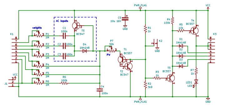
Capacitor C4, P7, T1 and T2 form a relaxation oscillator. The level that makes the switch trip is set by R1 and R2. C4 is charged by pulses arriving through D4, which combines the signals applied to the upper three (stimulus) inputs (K1, pins 7, 6 and 5).
C1/C2/C3, D4, T5 and C4 form a diode pump with three inputs (C1, C2 and C3). An incoming pulse charges C1 (or C2 or C3). D4 transfers this charge to C4, making the voltage over it increase. T5, an emitter follower, copies the voltage over C4 back to the anode of D4, which results in the next pulse being added to the previous. As a result, the voltage over C4 increases with every pulse. On an oscilloscope, the voltage over C4 looks like a staircase.
When the voltage over C4 becomes higher than the base voltage of T1 (the voltage set with R1 and R2 plus its B-E diode drop), T1 starts to conduct. A current starts to flow from C4 through P7 into the emitter of T1 and out of its collector into the base of T2, all the way to ground. This makes T2 conduct as well. As a result, it pulls the base of T1 much lower than its emitter voltage. T1 is now fully open and C4 can discharge quickly.
When the discharge current of C4 becomes low enough, T2 will stop conducting and the base of T1 jumps back to the voltage level set with R1 and R2. Because the voltage over C4 is almost zero, the base voltage of T1 is now much higher than its emitter voltage and therefore T1 too stops conducting. We are back where we started.
This particular configuration of T1 and T2 is sometimes referred to as a transistorized thyristor and was popular in the 1970s. It is important to note that T2 should not have too high a beta (hFE) value, otherwise it will keep conducting even when the discharge current is almost zero. An A- or B-type transistor will work well, but a C-type may be too sensitive. Therefore use a BC547A (or equivalent) for T2. For T5, also a BC547, the beta value doesn’t really matter, so it can be a BC547A too. This spares a line on the bill of materials.
Potentiometer P7 controls the discharging time of C4. When the value of P7 is small, the active-low pulse on R1/R2 is short. K2 provides a test point for it.
The signal on R1/R2 is buffered by PNP transistor T3. D1, D2 and D3 provide three active low outputs for the neuron. When T3 blocks, they are pulled high by R4. They are pulled low when T3 conducts. Similarly, when T3 blocks, T4 blocks too and the neuron’s active-high outputs (K3, pins 5, 6 and 7) are disconnected. When T3 conducts, T4 conducts too, and the outputs are pulled high. LED1 lights up to signal the pulse. What this means is that the outputs are low impedance when the neuron is firing a pulse and high impedance otherwise. This avoids two neurons influencing each other when driving the same neuron.
The two output types allow a neuron to stimulate another neuron or, on the contrary, to inhibit it. This is easier understood when looking at the neuron’s inputs. Here too are two types. The upper three ‘AC’ inputs connect to the diode pump as mentioned before. The lower three ‘DC’ inputs connect each through a weight potentiometer to C4. These inputs allow controlling the charge of C4 directly by either charging or discharging it (leaking).
The lower input (K1, pin 2) features jumper J1 to simplify connections for common cases. When pins 1 & 2 of J1 are shorted, potentiometer P6 provides an adjustable leak. With J1’s pins 2 & 3 shorted, P6 charges C4 and the neuron starts to oscillate. R6 ensures that oscillation occurs over the full range of P6.
To turn the AC inputs into DC inputs, replace C1, C2 and C3 by a diode (anode connected to the potentiometer), replace D4 by a wire bridge, and do not mount T5. The three diodes are required to prevent neuron inputs from influencing one another. If you replace C1, C2 and C3 by a wire bridge instead, you create more leak inputs.
The power supply is noncritical and can be anything from about 3.5 V to 15 V or even higher if you adapt C5 accordingly. The current consumption is mainly determined by the LED and is less than 1 mA for a 5 V supply.
PCB Design
Designs for both through-hole (THT) and SMD PCBs can be downloaded below. When using the SMD board, it may be useful to ask the board manufacturer to create a panel, e.g., 3 by 3, with V-grooves. This makes experimenting more convenient. See the attached photograph below.
Teaching a Neural Network
Unfortunately, I have no idea how to teach a neural network to do something useful. If you do, please leave a comment below.
Discussie (0 opmerking(en))